
G2LGAN + CNN (2025)
Two-stage GAN augmentation with MobileNetV2 handles class-imbalanced wafer map defect classification.
Benchmark architecture
INSPECTION & TEST
Wafer Inspection & Test
Metrology, defect inspection and electrical test across the whole line.
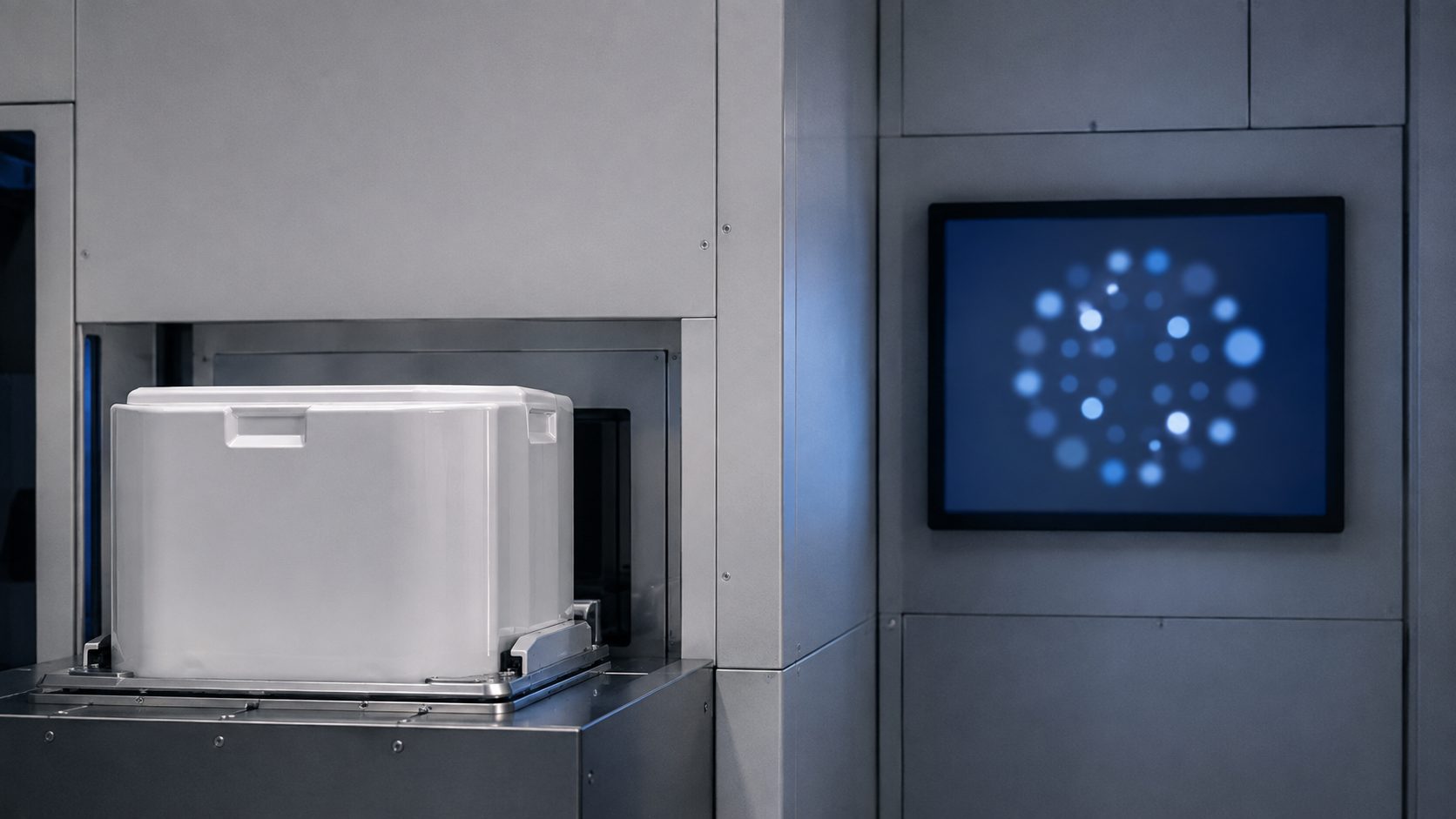
EQUIPMENT SCOPE
Focused on leading Japanese brands, covering electrical test and optical or laser inspection equipment.
SERVICES
AI INTEGRATION
The methods BETTER deploys and the third-party frontier architectures it benchmarks.
G2LGAN + CNN (2025)
Two-stage GAN augmentation with MobileNetV2 handles class-imbalanced wafer map defect classification.
Benchmark architecture
CNN-ESN (2026)
ResNet34 with an echo state network improves recognition robustness on noisy wafer maps.
Benchmark architecture
SEMVision H20 (2025)
Deep learning image classification, trained continuously in the fab, speeds up e-beam defect review.
Benchmark architecture
GPU real-time adaptive test
GPU-accelerated machine learning adapts the test flow in real time and shortens test time.
Benchmark architecture
KGD and outlier detection (GPR, conformal prediction)
Spatial modeling and conformal prediction sharpen known good die screening and outlier detection.
Benchmark architecture
InF-ATPG (2025)
FFR partitioning combined with QGNN and DQN optimizes test pattern generation.
Benchmark architecture
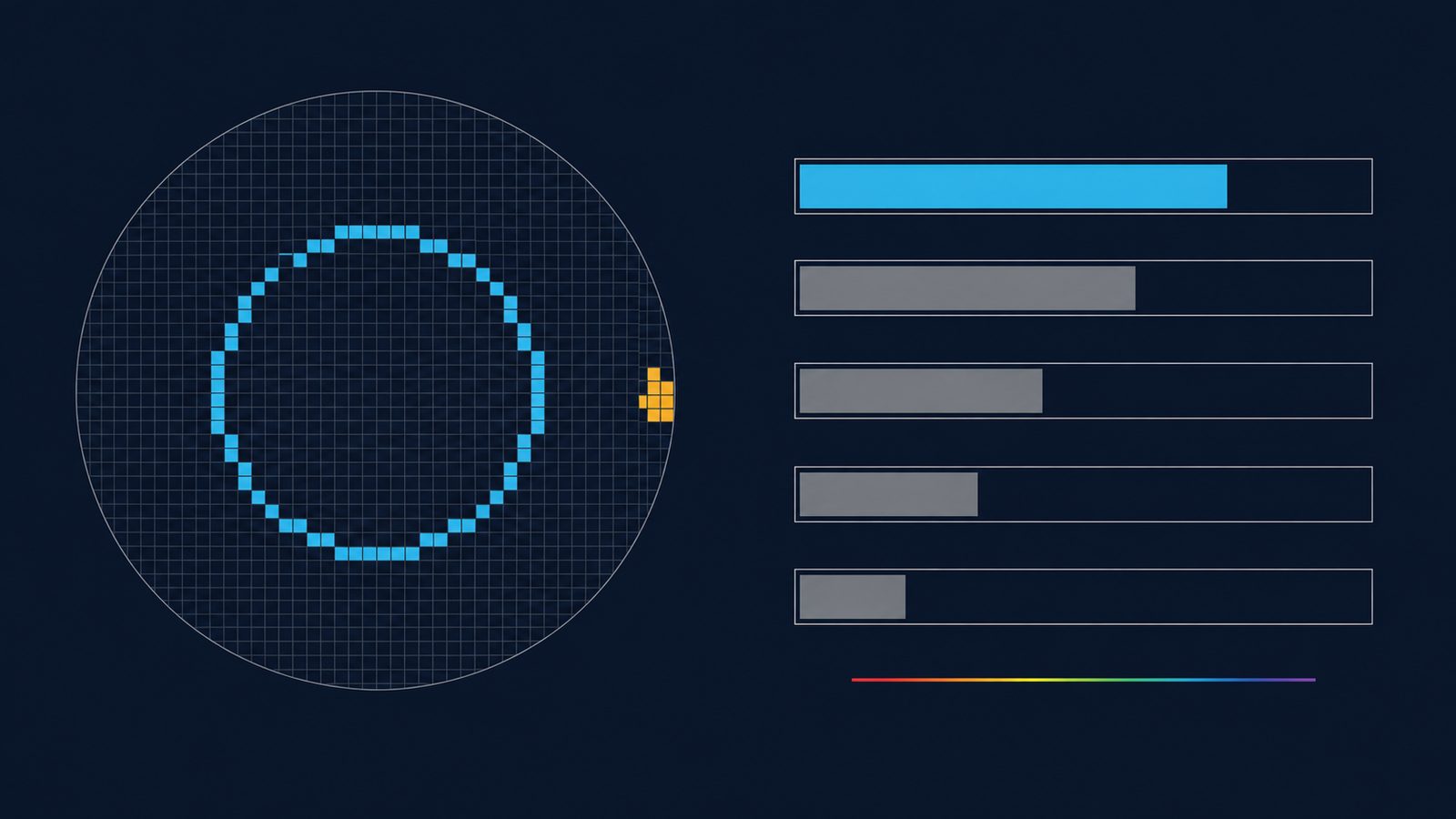
USE CASES
GET IN TOUCH
One point of contact from equipment selection through installation and AI integration.