EQUIPMENT & PROCESS
Equipment across nine process areas
Every area maps to leading Japanese brands and its own AI benchmark architectures.
PROCESS FLOW
How the areas connect
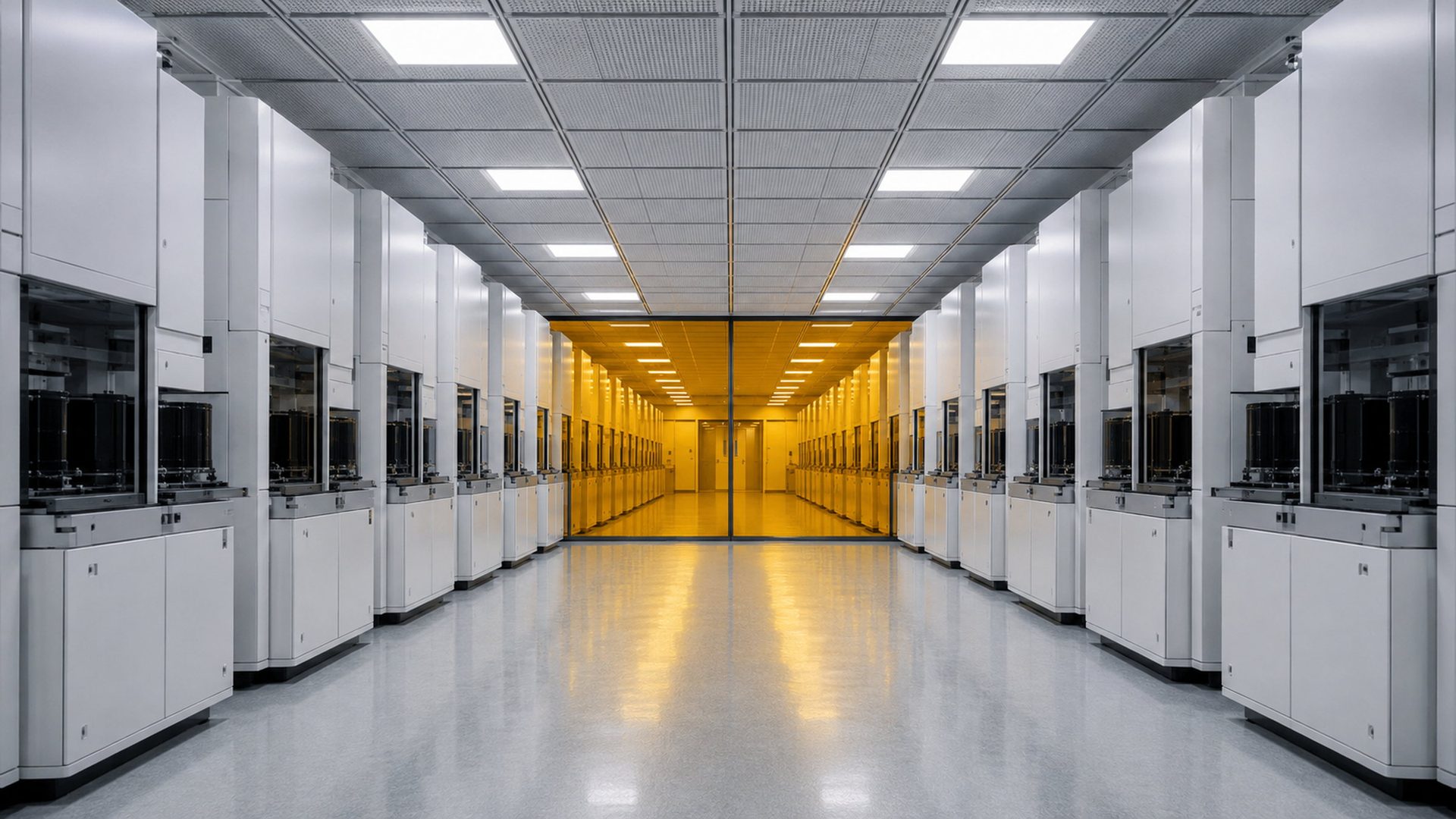
Wafer fabrication is a repeating cycle of stacked layers. The pattern is first formed on the photomask, then transferred to the wafer in lithography.
Etch defines the structure, CVD deposits thin films, bake controls the thermal budget, and ion implantation sets doping and electrical behavior.
CMP handles planarization, wafer cleaning suppresses particles and residue, and inspection runs through the whole line to provide feedback.
The nine areas feed one another, and variation in any one is amplified through the stack, so equipment and data strategy has to be consistent.
NINE AREAS
Equipment by process area
Select any area to see its equipment scope, services and AI integration.
01
Photolithography
Procurement, sales and maintenance of exposure tools and coat and develop tracks.
- NIKON
- CANON
- TEL
- DNS
View equipment
02
Dry & Plasma Etch
Procurement, sales and maintenance of etch equipment.
- TEL
- SAMCO
View equipment
03
CVD
Procurement, sales and maintenance of CVD equipment.
- KOKUSAI ELECTRIC (KE)
- MATSUSHITA
View equipment
04
Bake & Thermal
Procurement, sales and maintenance of bake and thermal equipment.
- KOKUSAI ELECTRIC (KE)
- TAZMO
View equipment
05
Ion Implant
Procurement, sales and maintenance of ion implantation equipment.
- ULVAC
- NISSIN
View equipment
06
CMP
Procurement, sales and maintenance of CMP equipment.
- EBARA
- ACCRETECH
View equipment
07
Wafer Clean & Dry
Procurement, sales and maintenance of wafer cleaning equipment.
- DNS
- TEL
View equipment
08
Inspection & Test
Procurement, sales and maintenance of inspection and test equipment.
- ADVANTEST
- LASERTEC
View equipment
09
Photomask
Procurement, sales and maintenance of photomask equipment.
- NUFLARE
- JEOL
View equipment
BETTER provides procurement, sales and maintenance services for the equipment brands listed above. Brand names are trademarks of their respective owners and are used for equipment identification only.
SERVICE COVERAGE
Services included in every area
- Procurement and tool selection
- De-installation, packing and cross-border shipping
- Move-in installation and tuning
- Maintenance and spare parts planning
- Process technology transfer
- Operation and maintenance training
- AI integration
GET IN TOUCH
Let's talk about your line
One point of contact from equipment selection through installation and AI integration.